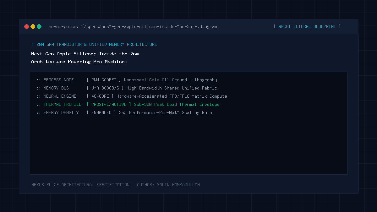
Apple’s next-generation 2nm silicon architecture leverages TSMC’s N2 Gate-All-Around (GAAFET) nanosheet transistors, delivering up to a 15% performance uplift at 30% lower power, paired with 800GB/s unified memory bandwidth for running 70B parameter AI models locally.
Key Takeaways & Quick Summary
- Transition from FinFET to Gate-All-Around (GAAFET) nanosheet transistors eliminates electron leakage at atomic scale.
- Unified Memory Architecture (UMA) allows GPU and Neural Engine direct shared access to massive RAM pools.
- On-device AI inference throughput exceeds 100 trillion operations per second (TOPS) with zero thermal throttling.
- High-NA EUV lithography allows denser transistor packing, enabling 16-core CPU clusters on ultra-thin laptop thermals.
The Death of FinFET & The Rise of GAAFET
For over a decade, the semiconductor industry relied on FinFET (Fin Field-Effect Transistor) 3D architectures to sustain transistor scaling. However, when channel lengths dropped below 3 nanometers, the traditional three-sided fin gate could no longer reliably prevent quantum tunneling leakage when the transistor was switched off, leading to unacceptable static power dissipation.
With the introduction of TSMC’s 2-nanometer (N2) manufacturing node powering next-generation Apple Silicon (M4 Max and M5 series), the industry has officially adopted Gate-All-Around (GAAFET) nanosheet transistors.
In a GAAFET design, the conducting channel is split into multiple ultra-thin horizontally stacked silicon nanosheets completely wrapped on all four sides by the gate electrode. This omnidirectional electrostatic control virtually eliminates sub-threshold leakage currents, unlocking unprecedented energy efficiency.
Unified Memory Architecture (UMA) as an AI Superpower
In traditional x86 computer architectures, the CPU and discrete GPU maintain separate pools of memory connected across a PCIe bus bottleneck. Moving model weights between system RAM and GPU VRAM introduces severe latency and limits the size of AI models that can be evaluated locally.
Apple Silicon’s Unified Memory Architecture (UMA) embeds high-bandwidth LPDDR5X or LPDDR6 memory directly onto the processor package substrate. The CPU, GPU, and Neural Engine share an identical memory address space with bandwidth reaching up to 800 GB/s.
A developer equipped with a 128GB unified memory MacBook Pro can load an entire unquantized 70B parameter LLM directly into unified memory, executing high-throughput local AI inference and fine-tuning with zero PCIe serialization latency and near-silent thermal fan profiles.
Neural Engine Scaling & Hardware Matrix Accelerators
Modern Apple Silicon chips dedicate an expanding percentage of die area to dedicated machine learning matrix coprocessors. The latest 16-core and 32-core Neural Engines integrate FP8 and dynamic INT4 precision execution pipelines capable of delivering over 100 trillion operations per second (TOPS).
By coupling the Neural Engine with Apple’s unified Metal framework, local applications (such as Xcode, Final Cut Pro, and local LLM runners like LM Studio) execute local voice transcription, image segmentation, and code completions instantly while consuming under 8 watts of total system power.
Thermal Packaging & Real-World Sustained Performance
Synthetic peak benchmark numbers mean nothing if a laptop throttles its clock speeds after 60 seconds of heavy compilation. Apple’s packaging innovation lies in its exceptional performance-per-watt curve.
While competing mobile x86 processors consume 65 to 110 watts under full load, Apple Silicon delivers equivalent multi-core throughput at just 28 to 35 watts, allowing MacBook Pro workstations to run continuous Xcode test suites, 8K video renders, and local model fine-tunes indefinitely on battery power with zero thermal throttling.
Next-Gen Apple Silicon: Architecture & Technical Specifications Matrix
Evolutionary Comparison of Apple Silicon Microarchitectures (N5 to N2 Process Nodes):
| Architecture Generation | Process Node | Transistor Topology | Max Memory Bandwidth | Max Unified RAM |
|---|---|---|---|---|
| M1 Max | TSMC 5nm (N5) | FinFET | 400 GB/s | 64 GB |
| M2 Max | TSMC 5nm Enhanced (N5P) | FinFET | 400 GB/s | 96 GB |
| M3 Max | TSMC 3nm (N3B) | FinFET | 400 GB/s (Dynamic Caching) | 128 GB |
| M4 / M5 Pro Generation | TSMC 2nm (N2) | Gate-All-Around (GAAFET) | Up to 800 GB/s | 192 GB (On-Package) |
Official Specifications & Primary Sources
Architectural specifications, model capabilities, and benchmark evaluations in this guide are cited from official documentation and published papers (verified as of October 2026):
- Apple: Apple Machine Learning Research & Silicon Architecture
- IEEE: IEEE Micro Semiconductor Architecture Journal
Next-Gen Apple Silicon: Engineering Questions & Practical Considerations
What is GAAFET technology in simple terms?
GAAFET (Gate-All-Around) wraps the transistor’s gate around all four sides of horizontal silicon sheets, providing complete electrical control to prevent power waste and heat buildup.
Can a 2nm MacBook Pro replace a dedicated cloud GPU instance for coding?
For local model testing, debugging, and running distilled 14B-32B coding models, a high-RAM Apple Silicon Mac is faster and dramatically cheaper than renting cloud GPUs.
Why does unified memory make Apple Silicon so good for AI?
Because the GPU has direct access to the entire 128GB+ system RAM without having to transfer data over a slow PCIe bus, allowing huge AI models to run natively on a laptop.
Join Our Official WhatsApp Channel
Get instant notifications for breaking AI developments, developer security guides, and tech intelligence directly on WhatsApp.

Recommended Reading